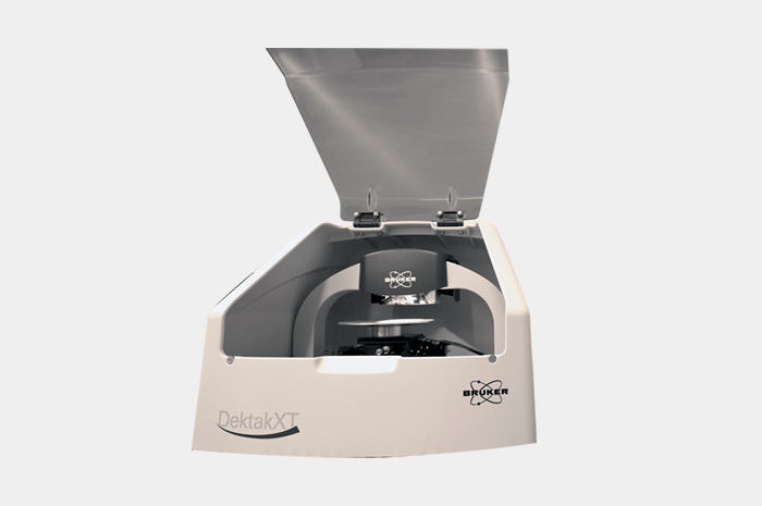
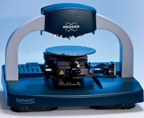
BRUKER Dektak-XT

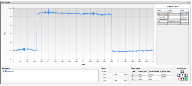
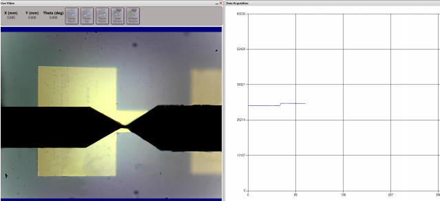
The sample is scanned by the probe, and the height difference and surface profile of the sample step can be calculated by using the principle of step height difference. It is mainly used for the thickness measurement of photoresist, SIO2, SI3N4, metal thin film, etc. and the depth measurement of dielectric etching Suitable for wafer and chip of 6inch and below.
Main Specifications
Scanning needle:
12.5um;
Scanning range:
50um~55mm;
Three test profile modes are available (hills, valleys, hills and valleys);
Test accuracy:
± 0.01um;
Maximum test step height:
524um.


